Selected Publications

Thumbnail of figure from publication
By Derric B. Syme, Jason M. Lund, Brian D. Jensen, Robert C. Davis, Richard R. Vanfleet, and Brian D. Iverson
Abstract:

The fabrication and examination of a porous silica thin film, potentially for use as an insulating thin film, were investigated. A vertically aligned carbon nanotube (CNT) forest, created by chemical vapor deposition (CVD), was used as scaffolding to construct the porous film. Silicon was deposited on the CNT forest using low-pressure CVD (LPCVD) and then oxidized to remove the CNTs and convert the silicon to silica for electrical or thermal passivation (e.g., thermal barrier). Thermal conductivity was determined using a 1D heat-transfer analysis that equated radiative heat loss in a vacuum with conduction through the substrate and thin film stack. A comparison of the surface temperature differences between a sample film and a reference of comparable thermal resistance enabled determination of the increase in the thermal resistance and of the thermal conductivity of the films. For film thicknesses of approximately 55 μm, the cross-plane thermal conductivity was found to be 0.054–0.071 W m–1 K–1 over 378–422 K. This thermal conductivity value is in the range of other silica aerogels and consistent with the low gravimetric density of 0.15 g cm–3 for the samples. The film is also relatively smooth and flat, with an average arithmetic mean roughness of 1.04 μm.

Thumbnail of figure from publication
By Basu R. Aryal, Dulashani R. Ranasinghe, Tyler R. Westover, Diana G. Calvopiña, Robert C. Davis, John N. Harb, and Adam T. Woolley
Abstract:

DNA-based nanofabrication of inorganic nanostructures has potential application in electronics, catalysis, and plasmonics. Previous DNA metallization has generated conductive DNA-assembled nanostructures; however, the use of semiconductors and the development of well-connected nanoscale metal—semiconductor junctions on DNA nanostructures are still at an early stage. Herein, we report the first fabrication of multiple electrically connected metal—semiconductor junctions on individual DNA origami by location-specific binding of gold and tellurium nanorods. Nanorod attachment to DNA origami was via DNA hybridization for Au and by electrostatic interaction for Te. Electroless gold plating was used to create nanoscale metal—semiconductor interfaces by filling the gaps between Au and Te nanorods. Two-point electrical characterization indicated that the Au—Te—Au junctions were electrically connected, with current—voltage properties consistent with a Schottky junction. DNA-based nanofabrication of metal—semiconductor junctions opens up potential opportunities in nanoelectronics, demonstrating the power of this bottom-up approach.

Thumbnail of figure from publication
By Parker D. Schnepf, Aaron Davis, Brian D. Iverson, Richard Vanfleet, Robert C. Davis, and Brian D. Jensen
Abstract:

Combining the resolution of conventional gas chromatography systems with the size factor of microGC systems is important for improving the affordability and portability of high performance gas analysis. Recent work has demonstrated the feasibility of high resolution separation of gases in a benchtop-scale short column system by controlling thermal gradients through the column. This work reports a microfabricated thermally controllable gas chromatographic column with a small footprint (approximately 6.25 cm²). The design of the 20 cm column utilizes 21 individually controllable thin film heaters and conduction cooling to produce a desired temperature profile. The reported device is capable of heating and cooling rates exceeding 8000 °C/min and can reach temperatures of 350 °C. The control methods allow for excellent disturbance rejection and precision to within +/- 1 °ree C. Each length of the column between heaters was demonstrated to be individually controllable and displayed quadratic temperature profiles. This paper focuses on the fabrication process and implementation of the thermal control strategy.

Thumbnail of figure from publication
By David Kane, Robert Davis, and Richard Vanfleet
Abstract:

Atomic layer deposition (ALD) of Al2O3 on tall multiwalled carbon nanotube forests shows concentration variation with depth in discrete steps. While ALD is capable of extremely conformal deposition in high aspect ratio structures, decreasing penetration depth has been observed over multiple thermal ALD cycles on 1.3 mm tall multiwalled carbon nanotube forests. Scanning electron microscopy imaging with energy dispersive x-ray spectroscopy elemental analysis shows steps of decreasing intensity corresponding to decreasing concentrations of Al2O3. A study of these steps suggests that they are produced by a combination of diffusion limited precursor delivery and the increase in precursor adsorption site density due to nuclei growing during the ALD process. This conceptual model has been applied to modify literature models for ALD penetration on high aspect ratio structures, allowing two parameters to be extracted from the experimental data. The Knudsen diffusion constant for trimethylaluminum (TMA) in these carbon nanotube forests has been found to be 0.3 cm2 s−1. From the profile of the Al2O3 concentration, the sticking coefficient of TMA in the TMA/water thermal ALD process was found to be 0.003.

Thumbnail of figure from publication
By Steven G. Noyce, Richard R. Vanfleet, and Robert C. Davis (et al.)
Abstract: Microscale porous carbon mechanical resonators were formed using carbon nanotube templated microfabrication. These cantilever resonators exhibited nanoscale porosity resulting in a high surface area to volume ratio which could enable sensitive analyte detection in air. These resonators were shown to be mechanically robust and the porosity could be controllably varied resulting in densities from 102 to 103 kg m−3, with pore diameters on the order of hundreds of nanometers. Cantilevers with lengths ranging from 500 μm to 5 mm were clamped in a fixture for mechanical resonance testing where quality factors from 102 to 103 were observed at atmospheric pressure in air.
Thumbnail of figure from publication
By Basu Ram Aryal, Tyler Westover, Dulashani R. Ranasinghe, DIana Gabriela Calvopiña, Bibek Uprety, John N. Harb, Robert C. Davis, and Adam T. Woolley
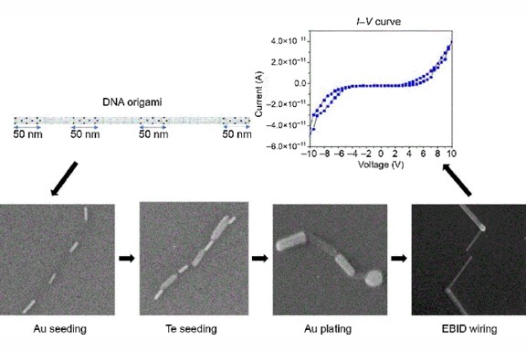
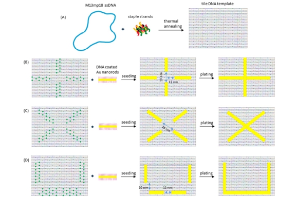
Abstract: Bottom-up nanofabrication is increasingly making use of self-assembled DNA to fabricate nanowires and potential integrated circuits, although yields of such electronic nanostructures are inadequate, as is the ability to reliably make electrical measurements on them. In this paper, we report improved yields and unprecedented conductivity measurements for Au nanowires created on DNA origami tile substrates. We created several different self-assembled Au nanowire arrangements on DNA origami tiles that are approximately 70 nm x 90 nm, through anisotropic growth of Au nanorods attached to specific sites. Modifications to the tile design increased yields of the final desired nanostructures as much as six fold. In addition, we measured the conductivity of Au nanowires created on these DNA tiles (~130 nm long, 10 nm diameter and 40 nm spacing between measurement points) with a four-point measurement technique that utilized electron beam induced metal deposition to form probe electrodes. These nanowires formed on single DNA origami tiles were electrically conductive, having having resistivities as low as 4.24 x 10⁻⁵ Ω m. . This work demonstrates the creation and measurement of inorganic nanowires on single DNA origami tiles as a promising path toward future bottom-up fabrication of nanoelectronics.