Welcome
 Welcome to the Colton group research homepage! The main research focus in our lab is the optical investigation of semiconductors and various semiconductor nanostructures. Some of the properties we measure are exciton binding energy, photoluminescence, spin lifetimes, and band gap energies. Electron spin lifetimes have particularly interesting applications to the field of quantum computing (see explanation below). For more information about our research, see the links to the left. Specifically, our research page describes several of the experiments we're currently working on. The basics of semiconductors page contains a brief introduction to the physics behind our experiments, and the optical experiments page describes some of the different techniques we use.
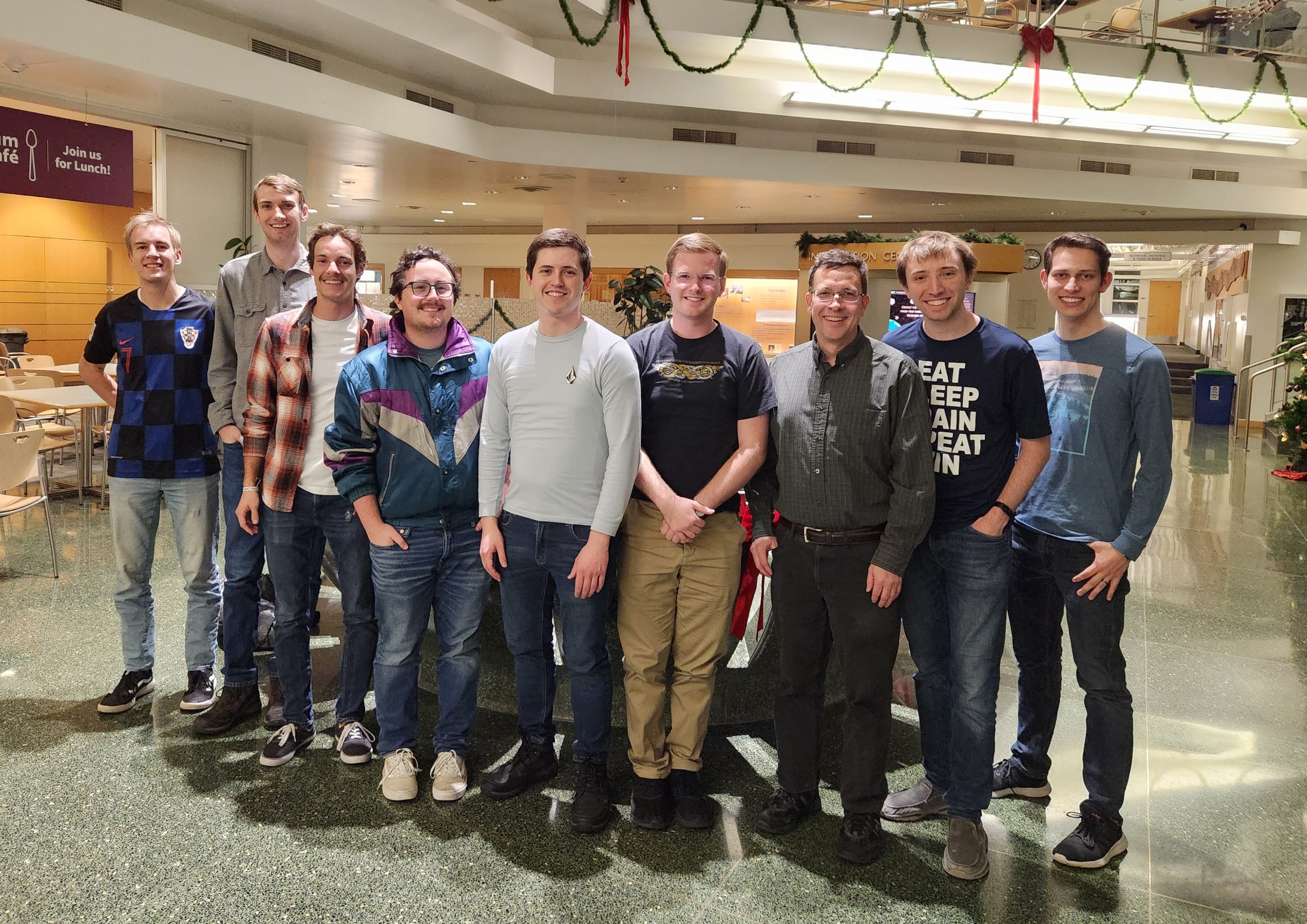 Colton Research Group, Dec, 2022
Physics Department Colloquium (3 Nov 2023)
Here's a colloquium I gave in Nov 2023 which explains some of our recent research on a particular class of hybrid organic-inorganic semiconductors, namely metal-halide perovskites.
Optical Investigations of Nanostructures
Our recent publications and research have been focused on materials for solar energy known as metal halide perovskites or hybrid organic-inorganic perovskites. These consist of a crystalline structure of inorganic layers made of metal and halogen (group VII) atoms which are a couple of nanometers thick, which are then attached to each other via organic linker molecules. These materials are of interest for their potential applications as light emmitters (LEDs) and solar cells. These perovskites have been improving in efficieny and show a lot of promise in those applications.
Analyzing the optical properties of the materials can help us understand what the electrons are doing inside the materials, which then can help advance the field and the effort to more efficient solar cells. We're studying properties such as the dielectric constant (which affects how much electrons inside the material are shielded from applied electric fields), and the binding energy between electrons and holes (a hole is the absence of an electron, and acts like a positive charge), and looking at how those properties change as the specific material compositions are varied.
Ferritin Nanoparticles
Our lab is currently investigating nanoparticle synthesis using the protein ferritin. Ferritin is a spherical protein that is especially useful for nanoparticle formation, because it offers a uniformly-sized shell in which to synthesize the nanoparticles. By varying the combinations of metals inside the ferritin shell, it is possible to create nanoparticles which have a variety of band gaps.
One of the primary applications for these nanoparticles is in multi-junction solar cells. Traditional single-junction solar cells have a maximum theoretical efficiency of only 33.7%; however, by using multiple layers of material, the maximum efficiency can be increased to over 80%. These layers need to have the proper band gaps in order to absorb the maximum amount of light, and we are searching for the proper combination of nanoparticles to use for a high-efficiency solar cell of this type.